1. Product Properties and Structural Integrity
1.1 Innate Features of Silicon Carbide
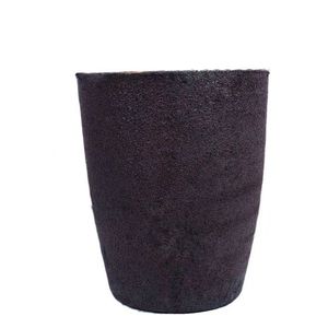
(Silicon Carbide Crucibles)
Silicon carbide (SiC) is a covalent ceramic substance made up of silicon and carbon atoms organized in a tetrahedral latticework structure, primarily existing in over 250 polytypic kinds, with 6H, 4H, and 3C being one of the most technically appropriate.
Its solid directional bonding conveys exceptional solidity (Mohs ~ 9.5), high thermal conductivity (80– 120 W/(m · K )for pure solitary crystals), and outstanding chemical inertness, making it among one of the most robust materials for extreme settings.
The broad bandgap (2.9– 3.3 eV) guarantees excellent electric insulation at area temperature level and high resistance to radiation damages, while its reduced thermal development coefficient (~ 4.0 × 10 ⁻⁶/ K) adds to exceptional thermal shock resistance.
These intrinsic homes are protected also at temperatures exceeding 1600 ° C, enabling SiC to maintain structural stability under prolonged exposure to molten metals, slags, and responsive gases.
Unlike oxide porcelains such as alumina, SiC does not respond easily with carbon or kind low-melting eutectics in minimizing ambiences, a vital benefit in metallurgical and semiconductor handling.
When produced into crucibles– vessels designed to consist of and warmth materials– SiC outperforms standard products like quartz, graphite, and alumina in both life expectancy and process dependability.
1.2 Microstructure and Mechanical Security
The performance of SiC crucibles is closely connected to their microstructure, which relies on the manufacturing technique and sintering ingredients used.
Refractory-grade crucibles are typically produced via response bonding, where permeable carbon preforms are infiltrated with molten silicon, creating β-SiC via the response Si(l) + C(s) → SiC(s).
This process generates a composite structure of main SiC with residual free silicon (5– 10%), which boosts thermal conductivity yet may restrict usage over 1414 ° C(the melting factor of silicon).
Alternatively, totally sintered SiC crucibles are made through solid-state or liquid-phase sintering using boron and carbon or alumina-yttria ingredients, achieving near-theoretical thickness and higher pureness.
These exhibit exceptional creep resistance and oxidation security however are extra pricey and tough to make in large sizes.
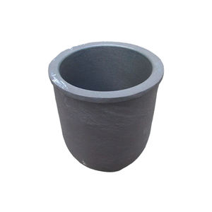
( Silicon Carbide Crucibles)
The fine-grained, interlocking microstructure of sintered SiC supplies outstanding resistance to thermal fatigue and mechanical disintegration, critical when taking care of liquified silicon, germanium, or III-V compounds in crystal growth procedures.
Grain border design, consisting of the control of secondary stages and porosity, plays an essential function in determining long-term toughness under cyclic heating and hostile chemical settings.
2. Thermal Efficiency and Environmental Resistance
2.1 Thermal Conductivity and Warmth Circulation
Among the specifying advantages of SiC crucibles is their high thermal conductivity, which makes it possible for fast and uniform warmth transfer throughout high-temperature processing.
In contrast to low-conductivity products like merged silica (1– 2 W/(m · K)), SiC successfully distributes thermal energy throughout the crucible wall, reducing local locations and thermal slopes.
This harmony is crucial in procedures such as directional solidification of multicrystalline silicon for photovoltaics, where temperature homogeneity straight impacts crystal quality and defect density.
The combination of high conductivity and reduced thermal development results in an incredibly high thermal shock specification (R = k(1 − ν)α/ σ), making SiC crucibles immune to fracturing during quick home heating or cooling down cycles.
This permits faster furnace ramp prices, enhanced throughput, and lowered downtime due to crucible failure.
Furthermore, the product’s capacity to withstand duplicated thermal cycling without significant destruction makes it ideal for batch handling in commercial heating systems running above 1500 ° C.
2.2 Oxidation and Chemical Compatibility
At elevated temperature levels in air, SiC undergoes passive oxidation, forming a protective layer of amorphous silica (SiO TWO) on its surface: SiC + 3/2 O TWO → SiO TWO + CO.
This glazed layer densifies at high temperatures, working as a diffusion barrier that slows down additional oxidation and protects the underlying ceramic structure.
Nonetheless, in reducing ambiences or vacuum cleaner problems– usual in semiconductor and metal refining– oxidation is suppressed, and SiC remains chemically secure versus liquified silicon, aluminum, and several slags.
It resists dissolution and reaction with liquified silicon approximately 1410 ° C, although prolonged exposure can result in small carbon pick-up or user interface roughening.
Crucially, SiC does not present metallic contaminations right into sensitive melts, an essential demand for electronic-grade silicon manufacturing where contamination by Fe, Cu, or Cr should be kept listed below ppb levels.
Nonetheless, care must be taken when processing alkaline planet metals or extremely reactive oxides, as some can corrode SiC at severe temperatures.
3. Production Processes and Quality Assurance
3.1 Fabrication Techniques and Dimensional Control
The manufacturing of SiC crucibles involves shaping, drying, and high-temperature sintering or seepage, with techniques chosen based upon required purity, dimension, and application.
Usual forming methods include isostatic pressing, extrusion, and slip casting, each supplying different degrees of dimensional accuracy and microstructural uniformity.
For huge crucibles made use of in photovoltaic or pv ingot spreading, isostatic pressing ensures constant wall density and density, decreasing the threat of crooked thermal development and failing.
Reaction-bonded SiC (RBSC) crucibles are economical and widely used in foundries and solar markets, though residual silicon restrictions maximum solution temperature level.
Sintered SiC (SSiC) versions, while extra expensive, deal superior pureness, toughness, and resistance to chemical attack, making them appropriate for high-value applications like GaAs or InP crystal development.
Precision machining after sintering may be needed to achieve tight resistances, particularly for crucibles made use of in upright gradient freeze (VGF) or Czochralski (CZ) systems.
Surface finishing is critical to lessen nucleation websites for flaws and make sure smooth melt flow during spreading.
3.2 Quality Assurance and Efficiency Recognition
Rigorous quality assurance is essential to make sure reliability and long life of SiC crucibles under demanding functional conditions.
Non-destructive analysis techniques such as ultrasonic screening and X-ray tomography are used to detect inner fractures, gaps, or density variants.
Chemical evaluation through XRF or ICP-MS validates reduced degrees of metal pollutants, while thermal conductivity and flexural toughness are measured to validate material consistency.
Crucibles are commonly based on substitute thermal cycling examinations before shipment to determine potential failure modes.
Set traceability and qualification are typical in semiconductor and aerospace supply chains, where component failing can cause pricey production losses.
4. Applications and Technological Impact
4.1 Semiconductor and Photovoltaic Industries
Silicon carbide crucibles play a crucial role in the manufacturing of high-purity silicon for both microelectronics and solar cells.
In directional solidification heating systems for multicrystalline solar ingots, big SiC crucibles act as the key container for molten silicon, enduring temperature levels above 1500 ° C for several cycles.
Their chemical inertness protects against contamination, while their thermal stability ensures consistent solidification fronts, leading to higher-quality wafers with less misplacements and grain borders.
Some suppliers layer the inner surface with silicon nitride or silica to better lower bond and facilitate ingot launch after cooling.
In research-scale Czochralski development of compound semiconductors, smaller SiC crucibles are used to hold thaws of GaAs, InSb, or CdTe, where very little reactivity and dimensional security are extremely important.
4.2 Metallurgy, Foundry, and Emerging Technologies
Beyond semiconductors, SiC crucibles are vital in steel refining, alloy preparation, and laboratory-scale melting procedures entailing light weight aluminum, copper, and precious metals.
Their resistance to thermal shock and erosion makes them perfect for induction and resistance heating systems in factories, where they last longer than graphite and alumina options by numerous cycles.
In additive manufacturing of responsive metals, SiC containers are utilized in vacuum cleaner induction melting to prevent crucible malfunction and contamination.
Arising applications include molten salt reactors and concentrated solar energy systems, where SiC vessels might contain high-temperature salts or fluid steels for thermal energy storage space.
With recurring advancements in sintering innovation and finish engineering, SiC crucibles are positioned to sustain next-generation materials processing, making it possible for cleaner, more effective, and scalable industrial thermal systems.
In summary, silicon carbide crucibles stand for an essential making it possible for innovation in high-temperature material synthesis, combining exceptional thermal, mechanical, and chemical efficiency in a solitary engineered part.
Their extensive fostering throughout semiconductor, solar, and metallurgical markets underscores their duty as a foundation of modern-day industrial porcelains.
5. Vendor
Advanced Ceramics founded on October 17, 2012, is a high-tech enterprise committed to the research and development, production, processing, sales and technical services of ceramic relative materials and products. Our products includes but not limited to Boron Carbide Ceramic Products, Boron Nitride Ceramic Products, Silicon Carbide Ceramic Products, Silicon Nitride Ceramic Products, Zirconium Dioxide Ceramic Products, etc. If you are interested, please feel free to contact us.
Tags: Silicon Carbide Crucibles, Silicon Carbide Ceramic, Silicon Carbide Ceramic Crucibles
All articles and pictures are from the Internet. If there are any copyright issues, please contact us in time to delete.
Inquiry us